80 kHz Modem
June 5, 2014
In today's lecture, I learned about the 80kHz modem and its corresponding circuit using a 4046 phase loop. This circuit utilizes two 4046 chips. In Figure 1 we can see the 80kHz modem circuit.
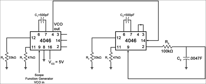
Figure 1: 80kHz Modem Circuit Utilizing the 4046 Phase Loop Configuration
The Loop filter is given by the following equation (Figure 2):
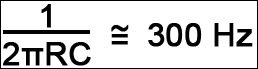
Figure 2: Equation to Loop Filter Relation to Frequency
Furthermore, the following table shows the relation between the Pull Lock Loop (PLL) frequency and the Voltage Controlled Oscillator (VCO) voltage (Table 1):
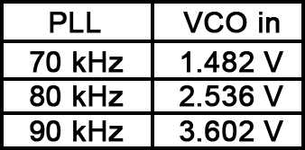
Table 1: Relation Between PLL Frequency and VCO in Voltage
To gain a better understanding of the 80kHz modem, we created a receiver circuit diagram and outlined the pins (In red) corresponding to the 4046 chip. This circuit diagram is shown in Figure 3.
Figure 3: Receiver Circuit Diagram Outlining Pins Corresponding to Figure 1
June 13, 2014
In today's lab I continued my work on the 80kHz modem. Below, you can see the configuration in which it was wired in Figure 4-5, below.
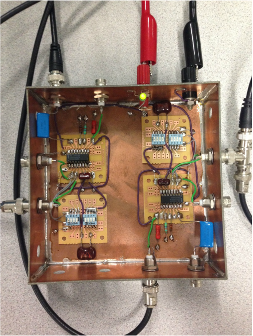
Figure 4: Top Down View of 80kHz Modem
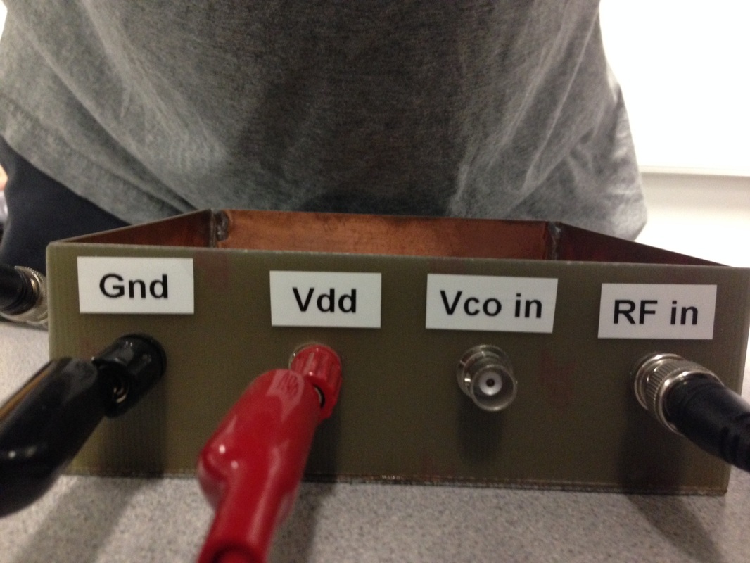
Figure 5: Final Side View Showing Ground, Vdd, VCO In and RF In Ports
With the above configuration in place, I used the oscilloscope's wave generator to generate spectras using the parameters in Table 2, below.
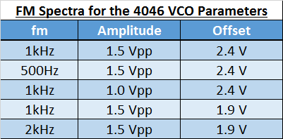
Table 2: Parameters for the Oscilloscope Waveform Generator
The spectras corresponding to the parameters in Table 2 are shown in Figures 6-10, below.
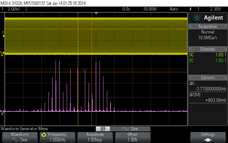
Figure 6: Spectra with the following parameters: fm=1kHz, Amplitude=1.5 Vpp, Offset=2.4 V
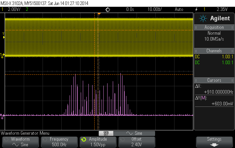
Figure 7: Spectra with the following parameters: fm=500Hz, Amplitude=1.5 Vpp, Offset=2.4 V
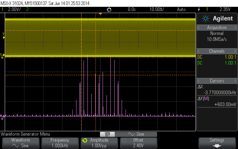
Figure 8: Spectra with the following parameters: fm=1kHz, Amplitude=1.0 Vpp, Offset=2.4 V
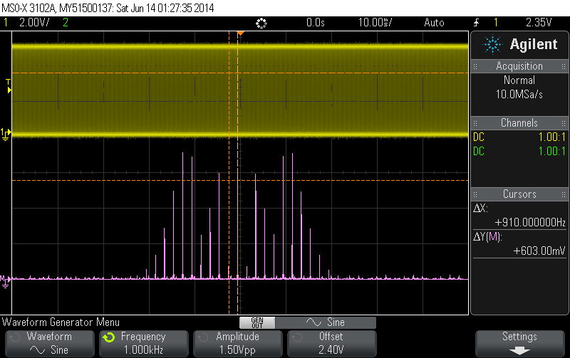
Figure 9: Spectra with the following parameters: fm=1kHz, Amplitude=1.5 Vpp, Offset=2.9 V

Figure 10: Spectra with the following parameters: fm=2kHz, Amplitude=1.5 Vpp, Offset=1.9 V
